Max Tolerance Stack-up: Strategies for PCBs and Blocks A, B & C

In summary, the individual tolerances for the holes had to be calculated in reference to the Datum which was located at the first hole.
  • #1
_Bd_
109
0
Hi,
I've been reading about stacking up tolerances. It's the first time in working with them. I understand the gist of it and I've seen a few simple examples however when I move onto my project I keep getting lost as I don't know what and where do they stack and if I should just add them up or Add them up and divide by two? (some of them are holes)

Here is the gist of it:
upload_2017-2-24_10-28-44.png


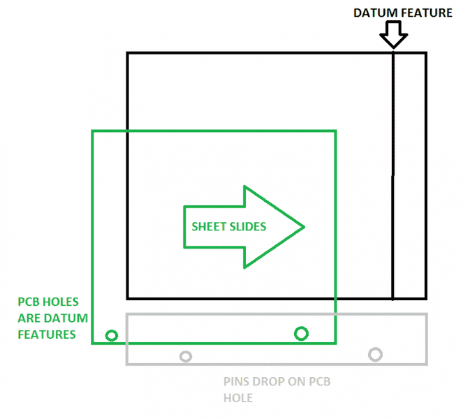
A flat PCB (a sheet looking thing with no components) slides into an aluminum block that has a datum feature on the side. the PCB is supposed to stop at that daturm. That datum is on Block A (Black).

Once the PCB is up against the stopper, Block B (grey) then drops on top of the PCB with some dowel pins.
The PCB mechanical drawing has those two holes as datum features with a tolerance of .003" (.075mm)

The thing is, Block B (grey) is mounted onto a big fiber-glass sheet (Let's calle it Block C).
Block A and Block B are mounted on the same sheet, and are assembled using screws.

My main question is:

- Would the tolerance analysis be done on Block C since that's where the alignment between block A and block B are done? or is it done on block A or block C or some sort of combination? and where does the PCB come into play?
 
Engineering news on Phys.org
  • #2
Let me ask you, your problem lists one datum feature with a tolerance of 3 thou. Furthermore the nature of the tolerance isn't specified. There's hole location with reference to the datum. There's hole size tolerance. There's a location tolerance between the holes. To name a few. What questions does this raise with you?
 
  • #3
My main concern is when the pin drops down how well aligned it will be with the hole on the PCB. I can start from the pin and work my way back, assuming the Pin's axis is the main daturm.
 
  • #4
_Bd_ said:
My main concern is when the pin drops down how well aligned it will be with the hole on the PCB. I can start from the pin and work my way back, assuming the Pin's axis is the main daturm.

Bd,

What is a Datum in terms of Quality Control? I don't think I'm giving an answer away with this one but Datum's are your references for the tolerances. You always start at the Datums. If you start anywhere else and work backwards to the Datum\reference what you will be stacking are the deviations of precision. More then likely sometime at during the early years of your career you will be tasked with designing a fixture for quality control. Your design will begin with the layout of the Datums identified on the part print. Datums usually are identified on a part print with a capital letter in a rectangle, box and sometimes a triangle. Unfortunately it's not always the case but Datum priority to the production of the part corresponds to the Datum letter. Tolerances for specifications from Datum "B" are in reference to Datum "A". Datum "C" is in reference to "B" which again is in reference to "A".

The way I understand your question, you are being asked to calculate the individual tolerances in reference to the Datums so that the hole locations match the arbitrary hole location dimension within .003. If I'm right with that it means you have to calculate tolerances for every dimension with reference to the dimension's priority Datum. Does that make sense?

Something to consider the location tolerance for the holes. There are 2 holes so should one of the holes actually be a Datum for the other or should the 2 together be a Datum? Should a Datum consist of 2 physically separated XY locations? Your drawing states the holes are Datum features. You should put some thought into the value of the holes as Datums. As drawn, as Datums what are they referencing? The Datum on the black block locates with a reference to the Y axis but are the holes the best choice for the X axis Datum? Consider a more complicated part to be QC'd. In terms of both the design of the fixture and calculating tolerances what serves you better, common and inclusive Datums or stand alone Datums that lack a "simple" reference to the Datum priority sequence?

When I turned 13 my father sent me to tool and die shop to start an apprenticeship. The very first job I was given I screwed up the layout on and I knew better. The job was machining a series of holes on a long titanium hinge of something like 15 feet. For some reason I laid out the holes by measuring distance from the previous hole instead of from the first hole layout. The tolerances were liberal but with something like 60 holes and carrying every hole deviation to the next location accumulatively and by the end I had the layout way off. My error was in not using a Datum. This happened long before the GD&T Standards but common sense and thinking first had been around for a while.

EDIT: Making the drop of the pin your last concern might help you?
 

Related to Max Tolerance Stack-up: Strategies for PCBs and Blocks A, B & C

1. What is the purpose of a Max Tolerance Stack-up for PCBs and Blocks A, B & C?

The purpose of a Max Tolerance Stack-up is to ensure that the dimensions and tolerances of all components in a circuit board or block are within the specified limits. This helps to prevent any potential errors or malfunctions in the final product.

2. How is a Max Tolerance Stack-up performed?

A Max Tolerance Stack-up is typically performed using software that allows for precise calculations and simulations of the dimensions and tolerances of all components. This can also be done manually by carefully measuring and calculating the dimensions of each component and their tolerances.

3. What are the main strategies for achieving a successful Max Tolerance Stack-up?

The main strategies for achieving a successful Max Tolerance Stack-up include carefully selecting components with appropriate tolerances, using the correct methods for assembling and mounting components, and performing thorough testing and inspection throughout the manufacturing process.

4. What are some common challenges when performing a Max Tolerance Stack-up?

Some common challenges when performing a Max Tolerance Stack-up include ensuring that all components are accurately measured and accounted for, dealing with variations in manufacturing processes, and ensuring that all components are within the specified tolerances.

5. What are the consequences of not performing a Max Tolerance Stack-up?

If a Max Tolerance Stack-up is not performed, there is a higher risk of errors and malfunctions in the final product. This can lead to costly rework and delays in production, as well as potential safety hazards if the circuit board or block is used in a critical application.

Similar threads

  • Introductory Physics Homework Help
Replies
2
Views
2K
  • Beyond the Standard Models
Replies
1
Views
3K
Back
Top