Current flow in NPN transistor

In summary, holes can be injected from the base to the emitter in an NPN transistor due to the difference in doping between the two regions. However, due to the abundance of free electrons in the emitter, injected holes are quickly destroyed. This results in a higher flow of electrons from the emitter to the collector, leading to current gain in the transistor. When an electron from the conduction band in the emitter falls into a hole in the base, it becomes a valence band electron and can either move to the positive lead of the battery or receive energy from the depletion region in the CB junction and exit the valence band. It is possible for both scenarios to occur.
  • #1
anhnha
181
1
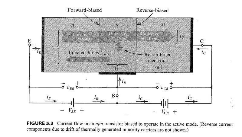
Here is an image show how currents flow in NPN transistor from Microelectronic Circuits by Sedra Smith:
attachment.php?attachmentid=59440&stc=1&d=1370916434.jpg

Can you explain more about injected holes (iB1)? I can't imagine how holes can flow into emitter (N type)
Is it possible to for holes to flow from base to emitter?
 

Attachments

  • Current flow.JPG
    Current flow.JPG
    52.8 KB · Views: 671
Physics news on Phys.org
  • #2
I think my main question is how holes diffuse from P type to N type semiconductor.
Can anyone help me explain it (how holes diffuse) in terms of electrons?
I can't imagine how holes can exist in N type by diffusion.
 
  • #3
It's been a few years so I'm a bit rusty but..

The base is +ve with respect to the emitter so you would expect holes to flow from base to emitter and electrons the other way. The number of holes injected into the emitter is a lot less than the number of electrons injected the other way due to the doping.

Due to the number of free electrons in the n-type emitter a hole injected there is not likely to go far before it meets an electron and is destroyed.

Since the base is short most of the electrons make it from the emitter to the collector and since only a few holes make it from base to emitter Ic>>Ib and the transitor has current gain.
 
  • Like
Likes 1 person
  • #4
Hi,
I am confused about this:
When we say that holes are injected from base to emitter it means that electrons in valence band (not electrons in conduction band) move from emitter to base.
Is this right?

And this is another question:
When an electron in conduction band from emitter falls into hole in base, it become electron in valence band. I wonder where the electron will go.
- the electron now is in valence band and it moves in valence band to positive lead of battery VBE
- the the electron now is in valence band and it moves in valence band to depletion region in CB junction and here it gets energy from VCB exits valence band and go into depletion region.

The first possibility is what I understand from the book but I wonder if the second is possible.
 
  • #5


I can provide some clarification on the concept of injected holes in an NPN transistor. In this type of transistor, the base region is made of a P-type semiconductor material, while the emitter and collector regions are made of N-type semiconductor material.

When a voltage is applied to the base-emitter junction, it creates a depletion region where there are no free charge carriers. However, when the voltage is increased beyond a certain threshold, it causes the injection of minority carriers (holes in the case of an NPN transistor) from the base into the emitter region.

These injected holes can then flow into the emitter region, which is N-type, as they are attracted to the region with an opposite charge. This flow of holes from the base to the emitter is what allows for the amplification of current in an NPN transistor.

So, to answer your question, yes, it is possible for holes to flow from the base to the emitter in an NPN transistor through the process of minority carrier injection. This is a fundamental principle in understanding the operation of transistors and is essential in the design and analysis of electronic circuits.

I hope this explanation helps to clarify the concept of injected holes in an NPN transistor. If you have any further questions, please don't hesitate to ask.
 

Related to Current flow in NPN transistor

1. What is an NPN transistor?

An NPN transistor is a type of bipolar junction transistor (BJT) that is commonly used in electronic circuits. It is composed of three layers - a thin layer of p-type semiconductor sandwiched between two layers of n-type semiconductor. The NPN acronym stands for the three layers - N (negative), P (positive), N (negative).

2. How does a current flow in an NPN transistor?

In an NPN transistor, current flows from the collector terminal to the emitter terminal. This current is controlled by the current flowing through the base terminal. When a small current is applied to the base, it amplifies and controls the larger current flowing from the collector to the emitter.

3. What is the function of the base terminal in an NPN transistor?

The base terminal in an NPN transistor is responsible for controlling the flow of current from the collector to the emitter. It acts as a switch, turning the transistor on and off by allowing or blocking the flow of current through the base-emitter junction.

4. How does the current amplification occur in an NPN transistor?

The current amplification in an NPN transistor occurs due to the transistor's structure and the flow of majority and minority charge carriers. When a small current is applied to the base, it controls the much larger current flowing from the collector to the emitter, resulting in an amplification of the current.

5. What are the applications of NPN transistors?

NPN transistors are commonly used in electronic circuits as amplifiers, switches, and voltage regulators. They are also used in digital logic circuits, audio amplifiers, and power supplies. NPN transistors are essential components in electronic devices such as computers, televisions, and smartphones.

Similar threads

  • Introductory Physics Homework Help
Replies
12
Views
282
Replies
5
Views
2K
  • Electrical Engineering
Replies
3
Views
824
  • Introductory Physics Homework Help
Replies
23
Views
3K
  • Introductory Physics Homework Help
Replies
8
Views
722
  • Electrical Engineering
Replies
5
Views
1K
  • Electrical Engineering
Replies
11
Views
1K
  • Introductory Physics Homework Help
Replies
8
Views
914
Replies
80
Views
3K
  • Engineering and Comp Sci Homework Help
2
Replies
59
Views
3K
Back
Top