What's the reason for modifying these amplifier circuits?

In summary, The conversation discusses the modification of a bjt amplifier with pure differential input signals to accommodate pure common mode signals. It is mentioned that the circuit is modified to exclude RE and include ro when finding the common mode input resistance. When asked about the reason for this modification, it is suggested that simplifying assumptions are being made. The conversation also delves into the analysis of the circuit without the small signal model and the implications of common mode signals on the voltage at x. Ultimately, the conversation concludes with a discussion on the exclusion of various components, such as re, in the calculation of the common input resistance.
  • #1
TheRedDevil18
408
1
If I have a bjt amplifier with pure differential input signals like this:
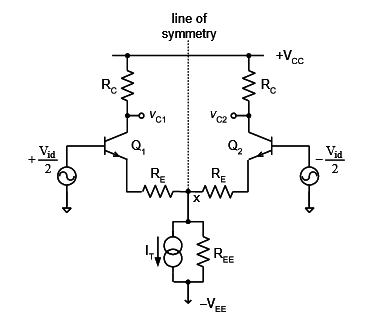
bjt diff.PNG


Now let's say I apply pure common mode signals to the same circuit, then why is the circuit above modified to this ?
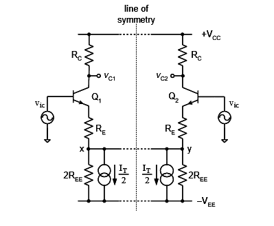
bjt common.PNG


Also when finding the Common Mode Input Resistance the circuit above excludes RE and includes ro, why ?
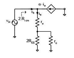
small signal.PNG
(finding input common mode resistance)
 
Engineering news on Phys.org
  • #2
For a pure common mode signal at both inputs both transistors are doing the same: Both will show slight increase of the collector currents.
OK - if they are doing the same, we can treat both transistor stages individually - however, in the first circuit the emittercurrent was split into two equal halfs. Therefore, each stage must have the same current IE as before: IT/2. And the same applies to REE. Putting both emitter nodes again together we gave 2REE||2REE=REE.
 
  • #3
LvW said:
For a pure common mode signal at both inputs both transistors are doing the same: Both will show slight increase of the collector currents.
OK - if they are doing the same, we can treat both transistor stages individually - however, in the first circuit the emittercurrent was split into two equal halfs. Therefore, each stage must have the same current IE as before: IT/2. And the same applies to REE. Putting both emitter nodes again together we gave 2REE||2REE=REE.

Ok yes I get that the two circuits are equivalent but then what if I analysed the circuit for the common mode signals without splitting the current source and REE (like first diagram), then for my small signal analysis I would neglect REE because the voltage at x is zero and I would get the wrong equation
 
  • #4
TheRedDevil18 said:
Also when finding the Common Mode Input Resistance the circuit above excludes RE and includes ro, why ?
(finding input common mode resistance)

Apparently they are making some simplifying assumptions. What do you get for the common mode input resistance?

By the way, is this homework?
 
  • #5
TheRedDevil18 said:
for my small signal analysis I would neglect REE because the voltage at x is zero and I would get the wrong equation
Why do you think the voltage at x would be zero? Can you verify this assumption?
 
  • #6
The Electrician said:
Apparently they are making some simplifying assumptions. What do you get for the common mode input resistance?

By the way, is this homework?

Ricm = Vic/ib
= (B+1)*ib*(2*REE//ro) / ib.......// means parallel combination
= (B+1)*(2*REE//ro)

This is not homework. This stuff is from the textbook and I just don't understand certain things
 
  • #7
LvW said:
Why do you think the voltage at x would be zero? Can you verify this assumption?

Because the symmetry ?
 
  • #8
TheRedDevil18 said:
Ricm = Vic/ib
= (B+1)*ib*(2*REE//ro) / ib.......// means parallel combination
= (B+1)*(2*REE//ro)

This is not homework. This stuff is from the textbook and I just don't understand certain things

Are you just using the simplified circuit shown in the third image in post #1?

What do you get if you analyze half the circuit shown in the second image of post #1? If I perform a nodal analysis on that half circuit, I get a much different result.
 
  • #9
TheRedDevil18 said:
Because the symmetry ?
Is there an ideal current source in the emitter leg? I don`t think so.
Hence, you have the classical common emiiter configuration with emitter feedback.
 
  • #10
The Electrician said:
Are you just using the simplified circuit shown in the third image in post #1?

What do you get if you analyze half the circuit shown in the second image of post #1? If I perform a nodal analysis on that half circuit, I get a much different result.

Yes, it's the last circuit in the post. I'm not too sure how to analyse it without the small signal model
 
  • #11
LvW said:
Is there an ideal current source in the emitter leg? I don`t think so.
Hence, you have the classical common emiiter configuration with emitter feedback.

In the book it says that the increase in signal current in one bjt is exactly matched by a decrease in the other hence the signal voltage at x is zero ?
 
  • #12
TheRedDevil18 said:
In the book it says that the increase in signal current in one bjt is exactly matched by a decrease in the other hence the signal voltage at x is zero ?

But his can`t be true for a common mode signal.
If the increase in T1 is identical to the decrease in T2 we have a differential signal without any common mode portion. Remember: In post#3 you speak abouta common-mode signal.
 
Last edited:
  • #13
TheRedDevil18 said:
Yes, it's the last circuit in the post. I'm not too sure how to analyse it without the small signal model

So analyze the half circuit shown as the second image in your first post using the small signal model. What do you get if you do that?
 
  • #14
The Electrician said:
So analyze the half circuit shown as the second image in your first post using the small signal model. What do you get if you do that?

It's the same answer that I posted above Ricm = (B+1)*(2*REE//ro)
 
  • #15
LvW said:
But his can`t be true for a common mode signal.
If the increase in T1 is identical to the decrease in T2 we have a differential signal without any common mode portion. Remember: In post#3 you speak abouta common-mode signal.

Ok, why is it not true for common mode signals ?
 
  • #16
TheRedDevil18 said:
View attachment 96070

Also when finding the Common Mode Input Resistance the circuit above excludes RE and includes ro, why ?

I can't tell you why they excluded RE, but when I solve for the common input Z, I get this (I included re in the model):

ComZ_1.png


If I delete the effect of various components, I get:

ComZ_2.png
 
  • #17
TheRedDevil18 said:
Ok, why is it not true for common mode signals ?

Because common-mode signals will cause the same current changes in both transistors (same direction).
 
  • #18
The Electrician said:
I can't tell you why they excluded RE, but when I solve for the common input Z, I get this (I included re in the model):

View attachment 96185

If I delete the effect of various components, I get:

View attachment 96186

They also neglected re, since it is much less than the parallel combination of 2REE and ro
 
  • #19
LvW said:
Because common-mode signals will cause the same current changes in both transistors (same direction).

Is the voltage at x measured across REE ?
 
  • #20
Have a look into your diagram how and where Vx is defined.
 
  • #21
When finding the common mode input resistance why is it 2*Ricm

They go on to say that 2*Ricm = Vic/ib but isn't that just for one amplifier or just Ricm ?
 
  • #22
TheRedDevil18 said:
When finding the common mode input resistance why is it 2*Ricm
They go on to say that 2*Ricm = Vic/ib but isn't that just for one amplifier or just Ricm ?
See my answer#17.
 

Related to What's the reason for modifying these amplifier circuits?

1. What is the purpose of modifying amplifier circuits?

The reason for modifying amplifier circuits is to improve the performance of the amplifier, such as increasing gain, reducing distortion, or increasing bandwidth. Modifications can also be made to customize the amplifier for a specific application or to troubleshoot and fix any issues with the circuit.

2. How do modifications affect the overall performance of the amplifier?

Modifications can have a significant impact on the performance of an amplifier. They can improve the frequency response, reduce noise, increase power output, and improve linearity. However, modifications must be carefully planned and executed to avoid damaging the circuit or causing unintended effects.

3. Can modifications be made to any type of amplifier?

Yes, modifications can be made to any type of amplifier, including tube, solid-state, and hybrid amplifiers. However, the specific modifications will vary depending on the type of amplifier and the desired outcome. It is important to have a thorough understanding of the circuit and its components before attempting any modifications.

4. What are some common modifications that can be made to amplifier circuits?

Some common modifications that can be made to amplifier circuits include changing the biasing, adjusting the feedback loop, adding or removing components, and changing the input or output stages. These modifications can improve the stability, gain, distortion, and frequency response of the amplifier.

5. Are there any risks associated with modifying amplifier circuits?

Yes, there are risks associated with modifying amplifier circuits. If modifications are not done correctly, they can damage the circuit or cause unwanted effects. It is important to have a thorough understanding of the circuit and to carefully plan and test any modifications before implementing them. It is also recommended to seek guidance from experienced professionals when making significant modifications to amplifier circuits.

Similar threads

  • Electrical Engineering
Replies
1
Views
1K
  • Electrical Engineering
Replies
20
Views
801
  • Electrical Engineering
Replies
3
Views
1K
  • Electrical Engineering
Replies
28
Views
3K
Replies
12
Views
1K
  • Electrical Engineering
Replies
3
Views
3K
  • Electrical Engineering
Replies
17
Views
1K
Replies
55
Views
3K
  • Electrical Engineering
Replies
4
Views
2K
Replies
2
Views
1K
Back
Top