Help with proper grounding with oscilloscope tracings

In summary, the inverter voltage is not clean and the ground is not connecting to the tank capacitor properly. The revised circuit using a comparator seems to be working better.
  • #1
imsmooth
152
13
I am having some issues when viewing tracings of my induction heater tank. It has to do with the grounding. First, I will explain the situation; then, I will ask the question.

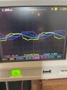
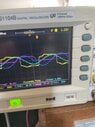
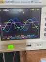
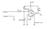
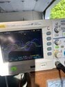
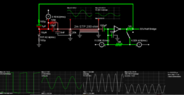
The images show the inverter voltage in yellow which results in a current in light blue. The dark blue is the 90 deg lagging tank capacitor voltage. The magenta is the tank capacitor voltage after it goes through a series 100k resistor that connects to two diode clamps connected to a 15v and 0v rail.

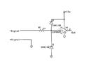
The power supply has a 15v and -15v rail and a center tap on the transformer for the ground/0v.
It uses a step down transformer with a center tap and goes through a bride rectifier. The output goes to a 15v and -15v regulators.

All images have:
a differential probe connected to the inverter voltage at x500 (yellow)
a standard x10 probe and its ground lead connected to the + and - ends of a current transformer (light blue)
a differential probe x500 connected to the tank capacitor (light blue)

This last part is the variable that I have a question with...

On image 1 there is a standard x10 probe with the signal input connected to the output of the diode clamp and the ground clip connected to the 0v rail. You can see how the yellow inverter voltage is not clean.

On image 2 I have connected an earth ground to the 0v rail. The probe's ground clip is now connected to the 0v rail and earth ground. Although the yellow tracing is not clean, it is better than the first image.

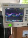
On image 3 I have disconnected the x10 probes ground clip from the 0v rail. Only the signal input is connected to the diode clamps. You can see the tracing is much cleaner.

These are grounding issues. How am I able to measure the magenta tracing in image three if I don't have the probe's ground lead connected to anything? My 0v rail is relative to the 15v rail. It is not necessarily at the same potential as earth ground. Are my signals in image 1 and 2 really not "clean" or is this an artifact from how I am not grounded properly? Why is my yellow tracing using a differential probe affected by my measurements with one of the standard probes?
 

Attachments

  • wave1.jpg
    wave1.jpg
    43 KB · Views: 50
  • wave2.jpg
    wave2.jpg
    46.3 KB · Views: 67
  • wave3.jpg
    wave3.jpg
    47.1 KB · Views: 61
Engineering news on Phys.org
  • #2
I think I got it to work correctly using a different circuit design. Still have some distortion on the yellow inverter tracing by having one end of the high voltage capacitor connected to the ground lead of the circuit board.
 

Attachments

  • wave1.jpg
    wave1.jpg
    42.5 KB · Views: 60
  • #3
imsmooth10 said:
I think I got it to work correctly using a different circuit design.
Perhaps you could attach a circuit diagram of the original and the revised circuit.
 
  • #4
The simple circuit below seems to give me the best, stable results, which I show with wave1. The 1M resistor limits the current since my capacitor can go as high as 750Vrms. The diode clamps keep it between 15v/0v. The inverter squares the signal. Since it is inverted I swapped the signal input polarities. I still have a less than clean signal on the yellow inverter tracing, but things seem good enough for me to put together a PCB with tight tracings and see what happens.

Circuit two uses a comparator to clean the signal. As you can see from tracing there is noise that gets into the output and I do not know how to get rid of it. It appears when the tank capacitor voltage gets high. Nothing changes if I attach earth ground to the system.

The scope probe is x10 and is connected to the output and the ground clip is attached to the power supply ground (same as the signal and emitter out).
 

Attachments

  • tank using hex inverter.jpg
    tank using hex inverter.jpg
    14.3 KB · Views: 57
  • tank using comparator.jpg
    tank using comparator.jpg
    17.8 KB · Views: 54
  • tracing using hex.jpg
    tracing using hex.jpg
    43.2 KB · Views: 55
  • wave_comparator.jpg
    wave_comparator.jpg
    41.7 KB · Views: 62
  • #5
Are all probes calibrated and accurate to get a flat line on gnd? and signals protected from crosstalk? The CMOS limiter is expected to perform best.
 
  • #6
Ground by definition is any 0 V reference with less error than you expect when measured against itself with ingress noise. ( eg. RF on Protective Earth gnd)

- So if you have grounding issues, measure it and show what your probe shows for ground. (both inputs.)
- Some grounds share unwanted currents, others are used to divert shield emissions to a protective earth ground for a differential pair.
- Often you only connect a shield to earth at one receiving end to avoid the ground loop.
If ground noise is still excessive, define what you expect and show how you measured it.

Another gnd issue is harmonic resonance from scope ground inductance on a fast rising step pulse ( usually > 20 MHz and can be filtered out on DSO filter option or reduce ground clip length to tip and coaxial ring.
 
  • Like
Likes DaveE
  • #7
imsmooth10 said:
Circuit two uses a comparator to clean the signal. As you can see from tracing there is noise that gets into the output and I do not know how to get rid of it. It appears when the tank capacitor voltage gets high. Nothing changes if I attach earth ground to the system.
You claim to have a ground problem, but your circuit does not show the power supply grounds, nor the signal grounds, that you are considering. Signals should not connect to supply grounds that carry circuit power, except at one point. You should differentiate between signal and power ground on the diagram.

The LM311 circuit you show has two clamping diodes with a 1 Meg limiter resistor. But why is one diode connected to the +15V supply, while the other diode is to ground? They should each be connected to a ±15V supply, or both to signal ground. That would give you switching symmetry about ground. If connected to supply rails, the diodes will have a minimum reverse voltage capacitance as the signal crosses zero, than if they were antiparallel to ground. At the same time, I expect the 1 Meg resistor terminals will be more of a capacitive divider than a resistor at that slew rate.
 
  • Like
Likes TonyStewart, DaveE and berkeman
  • #8
if you add ESR, ESL, C stray to a schematic, things will make more sense

- although ESL is commonly ~ 1 uH/m for any conductor, it varies with ln (l/w) (=len./width ratio of conductor)
- since effective series inductance (ESL) has an impedance X(f)=2pifL , 1uH/m means X(1MHz)= j 63 ohm/m per MHz for most wires as a ballpark estimate.
Stray capacitance in std. density PCB traces 10 mil (0.25mm) track, gap might be 1 pF/cm

for crosstalk- ESR might range from ESR*C = T from ~ X ns for microwave caps to > 100 us for Alum. e-caps and >1us for most low ESR e-caps about 1% of general purpose

ask if unfamiliar

- keep this crosstalk in mind when laying out the board with/without shields
- cable impedance and noise is preventing you from getting textbook waveforms.

- I think a better design will use an 500:1 RC divider to a remote FET buffer like an active electret mic. on coax, then convert current to voltage on PCB with R pullup.

You can get textbook waveforms before and after coax or STP wire with current mode and self-biased CMOS inverter to square up. CMOS Logic already has dual diode clamps with 50k R to Vdd and Vss. But you can add 10K in series for extra protection.

e.g. 10Meg||2pF: 20k||1nF => JFET > cable > R pullup.
 
  • #9
For giggles and kicks, here's my 500A 2.5 kV Induction heater 30Vdc self-resonant to 75 kHz with a 1 mohm half bridge. https://tinyurl.com/2qs592a2 The coil might be 1" copper tubing with cooling.

In theory that's about 1.5 MW
Note this is all based on the Q of RLC's shown with a 2m cable in between the LC tank and the amplifier with DC self-biasing to Vdd/2 and automatic self-resonant oscillation. No uC needed.

1684373233244.png
 

Attachments

  • 1684364726971.png
    1684364726971.png
    23.7 KB · Views: 47
Last edited:
  • #10
TonyStewart said:
For giggles and kicks, here's my 500A 2.5 kV Induction heater 30Vdc self-resonant to 75 kHz with a 1 mohm half bridge. https://tinyurl.com/2qs592a2 The coil might be 1" copper tubing with cooling.

In theory that's about 1.5 MW
Note this is all based on the Q of RLC's shown with a 2m cable in between the LC tank and the amplifier with DC self-biasing to Vdd/2 and automatic self-resonant oscillation. No uC needed.
After 30 ms it is 750 Arms >2 MW 3kVrms with 1kW losses in the bridge (0.05%). Is this big enuf :cool:
 
  • #11
Baluncore said:
The LM311 circuit you show has two clamping diodes with a 1 Meg limiter resistor. But why is one diode connected to the +15V supply, while the other diode is to ground? They should each be connected to a ±15V supply, or both to signal ground. That would give you switching symmetry about ground. If connected to supply rails, the diodes will have a minimum reverse voltage capacitance as the signal crosses zero, than if they were antiparallel to ground. At the same time, I expect the 1 Meg resistor terminals will be more of a capacitive divider than a resistor at that slew rate.
I tried it with both the -15v rail and 0v rail. Both "appeared" to give similar results so I went with the design that did not need a -15v source. I don't mind putting together another PCB using a 15v and -15v supply if you think it would give a "better" timing of the zero crossing. I may just do it to see if it matters. I just saw that the 15v/0v system worked.

I am still not sure what is going on inside the inverter chip and the comparator chip that the former one is immune to the noise.
 
Last edited by a moderator:
  • #12
Just so you can see what the unit can do I have a link to an old video suspending a chunk of copper and stainless steel using about 10kw. A PLL compares the phase of the inverter and the square wave signal (the one I have been asking these questions about). That output voltage from the PLL is analyzed by an arduino, raising or lowering the VCO to stay within resonance.

I'm not sure how the large professional systems maintain resonance. Does anyone know if they use a microprocessor or is it all just hardware?

 
  • #13
imsmooth10 said:
I am still not sure what is going on inside the inverter chip and the comparator chip that the former one is immune to the noise.
We cannot know either because we have no circuit diagram that shows the different grounds and connection paths.

imsmooth10 said:
I'm not sure how the large professional systems maintain resonance. Does anyone know if they use a microprocessor or is it all just hardware?
It is usually a self resonant oscillator. Non-magnetic conductive material inside the inductor reduces the inductance slightly. Capacitors are switched in or out, when they set it up, to get operation at about the right frequency.

The other technique is to have a parallel resonant tank with a separate induction coil. Without a metal load in the coil, the current and voltage are in quadrature, so no real energy is drawn from the tank circuit. The oscillator and heater coil are coupled via taps on the main tank.

Your circuit has a series resonant circuit, with your driver in series with the tank current. It would be more economic to have LC parallel resonance, with an inductor tap to your heating coil, since then the MOSFET would then not need to conduct the entire inductor current.

imsmooth10 said:
A PLL compares the phase of the inverter and the square wave signal (the one I have been asking these questions about). That output voltage from the PLL is analyzed by an arduino, raising or lowering the VCO to stay within resonance.
Then you could use the VCO of the PLL to drive the switch, which would eliminate the Arduino, hardware and software. Selection of the mixer type would determine the phase.
 
  • #14
Baluncore said:
You claim to have a ground problem, but your circuit does not show the power supply grounds, nor the signal grounds, that you are considering. Signals should not connect to supply grounds that carry circuit power, except at one point. You should differentiate between signal and power ground on the diagram.

The LM311 circuit you show has two clamping diodes with a 1 Meg limiter resistor. But why is one diode connected to the +15V supply, while the other diode is to ground? They should each be connected to a ±15V supply, or both to signal ground. That would give you switching symmetry about ground. If connected to supply rails, the diodes will have a minimum reverse voltage capacitance as the signal crosses zero, than if they were antiparallel to ground. At the same time, I expect the 1 Meg resistor terminals will be more of a capacitive divider than a resistor at that slew rate.
The above is true yet not the reason for your problems.

Both circuit schematics use the same diode clamps to +15V and 0V. Although the datasheet worst-case specs are 4pF at 0V where it is highest for the 1N4148 the nominal specs are < 1pF. But more importantly, it is the attenuation and phase shift of the signal that is critical at the input switching threshold. So indeed one might suspect the 0V reference of the LM311 to be worse than the Vdd/2 threshold for CMOS it would not account for the distorted signals shown which occur from different variations of harmonic resonances that affect amplitude and phase of each to create a distorted recurring wave shape. This means the distortion is due to things not shown in the schematic, like parasitic impedance of the cable from magnetic ingress of harmonic currents.

1684460456685.png

If one wishes to perfect this signal capture, one needs to show all physical and spectral properties of all conductors of the emitted wave and captured wave.

I apologize this is obvious to me but hard to communicate, but easy to capture by a good photographer. I will try to explain my part and expect similar effort if you want to resolve your issues.
1684459814561.png

1684460603723.png


1684460533892.png
The 4pF max from one diode would introduce almost 60 degrees phase shifts at 75 kHz and 8 dB attenuation, yet graphs are always typical and not worst case. Meanwhile, all CMOS devices already have 50 k current limiters on the inputs with 2 stages of Schottky diode pairs from Vdd and 0V. I sketched that on your schematics for the Hex inverter.

You do not need -15V , but there are better designs such as a balanced Instrument amplifier but the biggest problem is the unknown parasitic impedance in your cables from driver to sensor and the emission signals. This means , driver harmonic leakage, sensor uH/m, pF /m shielding effectiveness and common mode rejection to signal and ground from unbalanced impedance ( between signal vs ground return) and lack of Ferrite choke (CM filter) Shielded STP wires with balanced Differential input amplifiers have fewer problems.

You do not need a uC or a VCO
because my design is the easiest using positive AC feedback which creates an oscillator and this is a closed loop with gain > 1. (But you may use whatever works and is most reliable)

By the way, my design simulator works well because it is the simplest form of a PLL. The oscillator automatically shifts frequency until the phase shift is 360 or 0 degrees with gain > 1. For you to do similar you must answer all my questions and more. This is logically what you need but not physically. ( We need more specs to do the physics) .. and this is > 1 MW !

1684460198707.png


I have chosen ideal RLC parameters of for low loss in the LC tank circuit components, low loss in the driver and matched RC impedance attenuator suitable for this bandwidth. That is how I would change your design.
 
Last edited:
  • #15
I took your 400V yellow signal , hand drew it and displayed the FFT up to 30 harmonics in log amplitude with phase distortion computed (+/-180 deg)

1684461958454.png


FYI only to prove what I said about spectral impedance distortion.

1684461838677.png


1684462182031.png
 
  • #16
TonyStewart said:
The 4pF max from one diode would introduce almost 60 degrees phase shifts at 75 kHz and 8 dB attenuation, yet graphs are always typical and not worst case.
The 1 Meg resistor is excessive, a couple of resistors in series to withstand the voltage, while totalling between 47k and 100k, might be a better choice for a limiter, to give lower phase shift. Diodes have capacitance, but when it comes to picofarads, we must consider all the circuit wire capacitance.

TonyStewart said:
Meanwhile, all CMOS devices already have 50 k current limiters on the inputs with 2 stages of Schottky diode pairs from Vdd and 0V.
CMOS static protection does not have the power dissipation necessary to limit a circuit input voltage. A professional should never rely on input protection when designing circuits.
 
  • #17
Baluncore said:
The 1 Meg resistor is excessive, a couple of resistors in series to withstand the voltage, while totalling between 47k and 100k, might be a better choice for a limiter, to give lower phase shift. Diodes have capacitance, but when it comes to picofarads, we must consider all the circuit wire capacitance.CMOS static protection does not have the power dissipation necessary to limit a circuit input voltage. A professional should never rely on input protection when designing circuits.
Thanks again everyone for the help. This is a great exercise for me to be better at this. So what the above is saying is that the hex inverter has internal protection, but I should not rely on it and still use the external diodes. I have to also get some 5W 100k resistors.
 
  • #18
TonyStewart said:
The above is true yet not the reason for your problems.

Both circuit schematics use the same diode clamps to +15V and 0V. Although the datasheet worst-case specs are 4pF at 0V where it is highest for the 1N4148 the nominal specs are < 1pF. But more importantly, it is the attenuation and phase shift of the signal that is critical at the input switching threshold. So indeed one might suspect the 0V reference of the LM311 to be worse than the Vdd/2 threshold for CMOS it would not account for the distorted signals shown which occur from different variations of harmonic resonances that affect amplitude and phase of each to create a distorted recurring wave shape. This means the distortion is due to things not shown in the schematic, like parasitic impedance of the cable from magnetic ingress of harmonic currents.
Tony you have given me a lot to process.

Is this magnetic ingress on my oscilloscope cables or is this within the circuit under study?

When I got all the distortion this was using a breadboard. Do you think for the sake of comparison I should see what happens if I make a small PCB with the comparator circuit just to see what happens, or would you suspect I will get similar results? I am using fat tracings to minimize ESL and I am keeping them short.
 
Last edited by a moderator:
  • #19
Baluncore said:
The other technique is to have a parallel resonant tank with a separate induction coil. Without a metal load in the coil, the current and voltage are in quadrature, so no real energy is drawn from the tank circuit. The oscillator and heater coil are coupled via taps on the main tank.
I thought about a parallel design, but for some reason series seemed easier. Is the advantage of a parallel tank that I can use lower current MOSFETs?
 
  • #20
imsmooth10 said:
I thought about a parallel design, but for some reason series seemed easier. Is the advantage of a parallel tank that I can use lower current MOSFETs?
Yes. You can have other taps on the tank, or other windings with a different impedance, that do not need to conduct 100% of the circulating energy.
 
  • #21
Until you show the layout of what we are looking at , it is everything under test.
A parallel tank uses a high impedance BJT current source driver or a stepup transformer.

After all I wrote, I believe you are asking the wrong questions and not giving photos from my questions on your layout.
 
  • #22
Asking about proper grounding and your test(?) that showed "no difference?" is the wrong question.

1. State: { your overall purpose, Eng. Specs, Assumptions and skill level }
2. If you lack certain understanding of theory, learn it or ask questions about it or find topics or ask for key words to search
3. Design Approach:
  • a. Define goals (acceptance all criteriae, budget (time $)
  • b. Write Eng. Specs,
  • c. Find state of the art to match
  • d. Decide on { Design & Make OR Buy } then do it
repeat from a. and refine until done.

Don't get lost in the details of how (implementation specific) when a. and b. have not been done.

There are many examples of Induction heat, all with different metrics.
(power W, kW, MW), impedance Z(f) , frequency)
e.g.
1684496024856.png
 
Last edited:

1. What is grounding and why is it important in oscilloscope tracings?

Grounding refers to the process of connecting an electrical circuit or device to the earth or a reference point to establish a common voltage level. In oscilloscope tracings, proper grounding is crucial because it helps to eliminate any unwanted noise or interference that can affect the accuracy and reliability of the measurements.

2. How can I ensure proper grounding in my oscilloscope tracings?

To ensure proper grounding, first, make sure that the oscilloscope is plugged into a properly grounded outlet. Then, connect the ground clip of the oscilloscope probe to the ground point of the circuit or device being measured. It is also important to use a short and low-impedance ground wire to minimize any potential noise or interference.

3. What are some common signs of improper grounding in oscilloscope tracings?

Some common signs of improper grounding in oscilloscope tracings include a distorted or noisy waveform, inconsistent measurements, and unexpected fluctuations in the signal. These can be caused by improper grounding or a faulty ground connection.

4. Can I use a separate ground wire for grounding in oscilloscope tracings?

Yes, you can use a separate ground wire for grounding in oscilloscope tracings if the ground connection on the device being measured is not easily accessible. However, it is important to ensure that the separate ground wire is securely connected to the ground point and that it is as short and low-impedance as possible.

5. Are there any safety precautions I should take when working with oscilloscope tracings and grounding?

Yes, it is important to always follow proper safety precautions when working with oscilloscope tracings and grounding. This includes wearing appropriate protective gear, using insulated tools, and ensuring that the oscilloscope is turned off and unplugged before making any connections or adjustments.

Similar threads

  • Electrical Engineering
Replies
2
Views
4K
Back
Top