- #1
TJonline
- 26
- 1
- TL;DR Summary
- I'm posting a brief description of the operation of a PN junction (diode) and inviting anyone to give me their opinion of anything significant that I've missed or misunderstood. Thanks.
Unbiased circuit (no driving voltage source) **************
 Fig 1
Fig 1
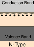
The N-type material has a tendency to donate electrons to the P-type (i.e. absorb holes from) across the PN junction via diffusion current exclusively within the conduction band of both materials. It does so after those electrons have made the small jump from the N-dopant's extrinsic donor energy level (black dots in Fig 1), through its extrinsic Fermi energy level (dotted line in Fig 1) and to the conduction band just above due to thermal energy/agitation.
That tendency (the Coulomb effect) is due to the relative abundance of electrons (majority carriers) in the N-type and is analogous to diffusion from high to low concentration in liquids. Before the join, the N-type is electrically neutral throughout with an equal number of electrons and protons for every atomic nuclei including its dopant nuclei.
Those nuclei contribute the donor energy level near the conduction band that accommodates its 'extra' electron that doesn't fit within its valence band that is already filled by it's own remaining four electrons and an electron from each its four silicon neighbors in the covalent bonds (shared electron pairs) of the silicon crystalline lattice to form a stable 'octet' (filled valence band).
 Fig 2
Fig 2
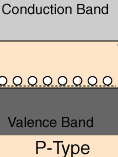
The P-type material has a tendency to donate holes to the N-type (i.e. accept electrons from) across the PN junction via diffusion current exclusively within the valence band of both materials. It does so after some of its valence electrons have made the small jump up from its valence band, through its Fermi energy level (dotted line in Fig 2) and to its extrinsic acceptor energy level (white circles in Fig 2) just above due to thermal energy/agitation.
The jump up of the electron can be viewed as a jump down of a hole from the acceptor band to the valence band. That tendency is again due to the Coulomb effect in the relative abundance of holes in the P-type. Before the join, the P-type is also electrically neutral throughout including its dopant nuclei. Those nuclei contribute the acceptor energy level just above the valence band such that there is one too few electrons for each dopant atom to complete an 'octet' with the help of its silicon neighbors.
The donor band is close to the valence band in the sense that it is relatively easy for holes in the valence band to move between all nuclei in the crystalline lattice and thermal agitation is sufficient to provide that energy. I use the terms 'energy' and 'band' more or less interchangeably (represented as the vertical direction in the included Figures).
 Fig 3
Fig 3
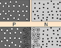
The two diffusion current components are additive in effect and continue until the number of excess electrons and negative ions in the P-type's conduction and valence bands (respectively) and the number of positive ions and holes in the N-type's valence and conduction bands (respectively) are great enough that any further increase in that generated charge imbalance (voltage) across the PN junction is countered by opposing drift current induced by that voltage.
At that point, the PN junction is at equilibrium with a constant, finite, intrinsic junction voltage and with (continuing) equal and opposite diffusion and drift currents. Essentially, that voltage is the result of the competition between the tendency of atoms to seek electrostatic stability (form a stable octet) acting over shorter distances and the electrical influence of the induced voltage acting over longer distances according to Ohm's law.
 Fig 4 (note that light and dark grey denote N and P type materials as opposed to energy levels/bands as in the other figures included herein)
Electrons and holes in the P-type's valence and conduction bands and the N-type's valence and conduction bands can also enter and leave both materials through their respective attached conductors. The conduction and valence bands in conductors overlap such that electrons are free to move between both, their Fermi levels being somewhere within that overlap (Fig 5).
 Fig 5
Fig 5
Forward bias driving voltage applied ********
 Fig 6
Fig 6
The applied voltage's positive terminal causes the conductor attached to the P-type to attract electrons from (i.e. inject holes into) the P-type's valence and conduction bands, and its negative terminal causes the conductor attached to the N-type to inject more electrons into the N-type's conduction and valence bands.
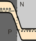
If that forward bias voltage is greater than the junction voltage (i.e. is able to resupply all lost electrons from the N-type and resupply lost holes from the P-type), then the junction voltage is overcome (Fig 6) and current continuously flows through the diode from attached conductor to attached conductor.
Reverse bias driving voltage applied ********
 Fig 7
Fig 7
The applied voltage's negative terminal causes the conductor attached to the P-type to inject electrons into (i.e. absorb holes from) its valence and conduction bands, and its positive terminal causes the conductor attached to the N-type to absorb holes from the N-type's conduction and valence bands, increasing the depletion voltage (Fig 7), and continuing until diffusion and drift currents are again equal and opposite at a new equilibrium such that the driving voltage is exactly opposed by the depletion voltage (like two batteries in series and their positive terminals in contact) and no net current flows through the circuit.
***********************
* Do the reverse bias injected charges migrate towards the depletion region and if so, by what mechanism? Or does the depletion region actually extend linearly across the entirety of the diode from attached conductor to attached conductor?
* Electrons occasionally fall from the conduction band to the valence band, resulting in the annihilation of an electron/hole pair and the emission of a photon (the basis of LEDs). Electrons occasionally leap from the valence band to the conduction band after absorption of a photon resulting in an electron/hole pair (the basis of solar cells). In a garden variety diode the rate at which those occur is insignificant. Those are relatively high energy interactions (as opposed to low energy interactions like thermal effects and voltage and current flow in wires and circuits) such that only certain photons have sufficient energy to produce them according to the quantum model of atoms in which low energy infrared photons generally don't have sufficient energy to induce anything interesting at all (except heat).
* Think of the Fermi level as the surface of a sea in a water analogy. The body of the sea and its surface are all the occupied atomic energy states at the lowest energy levels that their associated electrons can find, just as water always seeks a local depression (pool) below which surface topology dictates that water can flow no further. The Pauli Exclusion Principle dictates that no two electrons can occupy the same energy state, just as water molecules can't occupy the same space. Ripples upon that surface are analogous to low energy thermal and other effects. Quantum leaps (photonic effects) are 'unusual' events akin to a rock thrown into the surface that can sometimes induce a splash, or a water drop falling from a significant height causing another drop to pop up in response and inevitable ripples as well, since most all dynamic/energetic phenomena create or absorb some heat energy as a byproduct and are thus less than perfectly efficient.
* The Figures were borrowed from the HyperPhysics website, which I highly recommend and am sure many of you are already familiar with.
* Here is a Windows RTF version that anyone may feel free to mark up as they please. I only ask that you do so with strikethroughs and with red color to suggest what to omit or modify, leaving the original text. Thanks.
http://afafa.org/Unlinked/Diode_model_notes.rtf
The N-type material has a tendency to donate electrons to the P-type (i.e. absorb holes from) across the PN junction via diffusion current exclusively within the conduction band of both materials. It does so after those electrons have made the small jump from the N-dopant's extrinsic donor energy level (black dots in Fig 1), through its extrinsic Fermi energy level (dotted line in Fig 1) and to the conduction band just above due to thermal energy/agitation.
That tendency (the Coulomb effect) is due to the relative abundance of electrons (majority carriers) in the N-type and is analogous to diffusion from high to low concentration in liquids. Before the join, the N-type is electrically neutral throughout with an equal number of electrons and protons for every atomic nuclei including its dopant nuclei.
Those nuclei contribute the donor energy level near the conduction band that accommodates its 'extra' electron that doesn't fit within its valence band that is already filled by it's own remaining four electrons and an electron from each its four silicon neighbors in the covalent bonds (shared electron pairs) of the silicon crystalline lattice to form a stable 'octet' (filled valence band).
The P-type material has a tendency to donate holes to the N-type (i.e. accept electrons from) across the PN junction via diffusion current exclusively within the valence band of both materials. It does so after some of its valence electrons have made the small jump up from its valence band, through its Fermi energy level (dotted line in Fig 2) and to its extrinsic acceptor energy level (white circles in Fig 2) just above due to thermal energy/agitation.
The jump up of the electron can be viewed as a jump down of a hole from the acceptor band to the valence band. That tendency is again due to the Coulomb effect in the relative abundance of holes in the P-type. Before the join, the P-type is also electrically neutral throughout including its dopant nuclei. Those nuclei contribute the acceptor energy level just above the valence band such that there is one too few electrons for each dopant atom to complete an 'octet' with the help of its silicon neighbors.
The donor band is close to the valence band in the sense that it is relatively easy for holes in the valence band to move between all nuclei in the crystalline lattice and thermal agitation is sufficient to provide that energy. I use the terms 'energy' and 'band' more or less interchangeably (represented as the vertical direction in the included Figures).
The two diffusion current components are additive in effect and continue until the number of excess electrons and negative ions in the P-type's conduction and valence bands (respectively) and the number of positive ions and holes in the N-type's valence and conduction bands (respectively) are great enough that any further increase in that generated charge imbalance (voltage) across the PN junction is countered by opposing drift current induced by that voltage.
At that point, the PN junction is at equilibrium with a constant, finite, intrinsic junction voltage and with (continuing) equal and opposite diffusion and drift currents. Essentially, that voltage is the result of the competition between the tendency of atoms to seek electrostatic stability (form a stable octet) acting over shorter distances and the electrical influence of the induced voltage acting over longer distances according to Ohm's law.
Electrons and holes in the P-type's valence and conduction bands and the N-type's valence and conduction bands can also enter and leave both materials through their respective attached conductors. The conduction and valence bands in conductors overlap such that electrons are free to move between both, their Fermi levels being somewhere within that overlap (Fig 5).
Forward bias driving voltage applied ********
The applied voltage's positive terminal causes the conductor attached to the P-type to attract electrons from (i.e. inject holes into) the P-type's valence and conduction bands, and its negative terminal causes the conductor attached to the N-type to inject more electrons into the N-type's conduction and valence bands.
If that forward bias voltage is greater than the junction voltage (i.e. is able to resupply all lost electrons from the N-type and resupply lost holes from the P-type), then the junction voltage is overcome (Fig 6) and current continuously flows through the diode from attached conductor to attached conductor.
Reverse bias driving voltage applied ********
The applied voltage's negative terminal causes the conductor attached to the P-type to inject electrons into (i.e. absorb holes from) its valence and conduction bands, and its positive terminal causes the conductor attached to the N-type to absorb holes from the N-type's conduction and valence bands, increasing the depletion voltage (Fig 7), and continuing until diffusion and drift currents are again equal and opposite at a new equilibrium such that the driving voltage is exactly opposed by the depletion voltage (like two batteries in series and their positive terminals in contact) and no net current flows through the circuit.
***********************
* Do the reverse bias injected charges migrate towards the depletion region and if so, by what mechanism? Or does the depletion region actually extend linearly across the entirety of the diode from attached conductor to attached conductor?
* Electrons occasionally fall from the conduction band to the valence band, resulting in the annihilation of an electron/hole pair and the emission of a photon (the basis of LEDs). Electrons occasionally leap from the valence band to the conduction band after absorption of a photon resulting in an electron/hole pair (the basis of solar cells). In a garden variety diode the rate at which those occur is insignificant. Those are relatively high energy interactions (as opposed to low energy interactions like thermal effects and voltage and current flow in wires and circuits) such that only certain photons have sufficient energy to produce them according to the quantum model of atoms in which low energy infrared photons generally don't have sufficient energy to induce anything interesting at all (except heat).
* Think of the Fermi level as the surface of a sea in a water analogy. The body of the sea and its surface are all the occupied atomic energy states at the lowest energy levels that their associated electrons can find, just as water always seeks a local depression (pool) below which surface topology dictates that water can flow no further. The Pauli Exclusion Principle dictates that no two electrons can occupy the same energy state, just as water molecules can't occupy the same space. Ripples upon that surface are analogous to low energy thermal and other effects. Quantum leaps (photonic effects) are 'unusual' events akin to a rock thrown into the surface that can sometimes induce a splash, or a water drop falling from a significant height causing another drop to pop up in response and inevitable ripples as well, since most all dynamic/energetic phenomena create or absorb some heat energy as a byproduct and are thus less than perfectly efficient.
* The Figures were borrowed from the HyperPhysics website, which I highly recommend and am sure many of you are already familiar with.
* Here is a Windows RTF version that anyone may feel free to mark up as they please. I only ask that you do so with strikethroughs and with red color to suggest what to omit or modify, leaving the original text. Thanks.
http://afafa.org/Unlinked/Diode_model_notes.rtf
Last edited by a moderator: