Can you explain this amplifier circuit to me?

In summary, the current through TR2 is limited and it doesn't appear to have any real purpose in this circuit.
  • #1
wannab
32
1
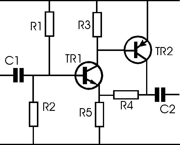
I just want to know what you think (in order of when you think it) when you look at this circuit. I'll post what I think.
transistor_2_device_amp.gif


1) without input: Current goes through R1 and TR1 which allows more current to flow through R3, R4, C2 and R5 and to TR2. The current through TR2 inhibits the current that was already flowing through it to the output.
2) with input: slightly more current goes through TR1 some of which goes to the output

As you can see it's fairly limited. I don't really know what the capacitors do here.
 
  • Like
Likes Omegatron
Engineering news on Phys.org
  • #2
That circuit would appear to have some issues. Where is it from? What is it supposed to be used for?
 
  • #3
Think of the transistors as voltage controlled resistors. E.G. When there is a voltage between the base and emitter of TR1, the switch starts to turn on (i.e. the resistance between the collector and emitter lowers) and current flows through TR1 from the collector to the emitter. So you have th think about this in terms of Ohm's Law. I.e you have to consider all three variables: current, voltage and resistance.

C1 is an input filter which blocks DC but passes an AC voltage to the base of NPN transistor TR1. R1 and R2 form a voltage divider that generates a fixed DC voltage which DC biases the base of TR1. When an AC signal is applied at the input, the passed AC signal adds with the DC bias voltage and hence the instantaneous voltage at the base of TR1 vibrates up and down around the DC bias voltage.
Then the instantaneous resistance of the collector-emitter path of TR1 changes in sync with the AC signal.

R3, R5, and the instantaneous collector-emitter resistance of TR1 form a second voltage divider circuit. Therefore the voltage at the collector varies as a function of the instantaneous resistance of the collector-emitter path of TR1. Resistors R1, R2, R3 and R5 control the amount of current flowing is both the base-emitter path and the collector-emitter paths of TR1. Typically the values are selected so that more current flows through the collector-emitter path than through the base-emitter path. Hence this circuit is a current amplifier circuit. In voltage terms, we could say that the instantaneous voltage at the collector of TR1 (i.e. the voltage across R3), varies more than the instantaneous voltage at the base.

However, it is also possible to set the values of the resistors to produce a gain of 1. In this case, the current through the collector-emitter of TR1 is higher that the base-emitter current but the voltages are identical. The circuit is purely a current amplifier. This circuit is frequently used to drive transmission lines longer than a few feet by providing more current to the transmission line.

Note that the voltages at the emitter-base and collector-emitter circuit paths are 180 deg. out of phase.

With respect to TR2, remember that it is a PNP transistor. It's resistance is highest when the base-emitter voltage is 0. This occurs when the base is at V+. In the NPN transistor TR1, the base voltage would be 0.

C2 is an output filter that functions exactly as the input filter - the AC signal passes but the DC signal is blocked.

With that info, how about if you try to figure out how TR2 works in this circuit? Think about it, post a response and I will fill in any blanks still left over.
 
Last edited:
  • #4
Think of the transistors as voltage controlled resistors. E.G. When there is a voltage between the base and emitter of TR1, the switch starts to turn on (i.e. the resistance between the collector and emitter lowers) and current flows through TR1 from the collector to the emitter. So you have th think about this in terms of Ohm's Law. I.e you have to consider all three variables: current, voltage and resistance.

C1 is an input filter which blocks DC but passes an AC voltage to the base of NPN transistor TR1. R1 and R2 form a voltage divider that generates a fixed DC voltage which DC biases the base of TR1. When an AC signal is applied at the input, the passed AC signal adds with the DC bias voltage and hence the instantaneous voltage at the base of TR1 vibrates up and down around the DC bias voltage.
Then the instantaneous resistance of the collector-emitter path of TR1 changes in sync with the AC signal.

R3, R5, and the instaneous collector-emitter resistance of TR1 form a second voltage divider circuit. Therefore the voltage at the collector varies as a function of the instantaneous resistance of the collector-emitter path of TR1. Resistors R1, R2, R3 and R5 control the amount of current flowing is both the base-emitter path and the collector-emitter path of TR1. Typically the values are selected so that more current flows through the collector-emitter path than through the base-emitter path. Hence this circuit is a current amplifier circuit. In voltage terms, we could say that the instantaneus voltage at the collector of TR1 (i.e.) the voltage across R3, varies more than the iunstantaneous voltage at the base.

However, it is also possible to set the values of the resistors to produce a gain of 1. In this case, the current through the collector-emitter of TR1 is higher that the base-emitter current but the voltages are identical. The circuit is purely a current amplifier. This circuit is frequently used to drive transmission lines longer than a few feet by providing more current to the transmissin line.

Note that the voltages at the emitter-base and collector-emitter circuit paths are 180 deg. out of phase.

With respect to TR2, remember that it is an PNP transistor. It's resistance is highest when the base-emitter voltage is 0. This occurs when the base is at V+. In the NPN transistor the base voltage would be 0.

C2 is an output filter that functions exactly as the input filter - the AC signal passes but the DC signal is blocked.

With that info, how about if you try to figure out how TR2 works in this circuit? Think about it, post a response and I will fill in any blanks still left over.
 
  • #5
I think it's a form of what used to be called a Complementary Feedback Pair - which gives high gain and low output impedance. It's a bit like the more familiar Darlington Pair which uses two npn or two pnp transistors for the same effect. I seem to remember that configuration was sometimes used as one half of a complimentary Audio output stage when only one type of high power transistor was available (or just for the hell of it).

It certainly isn't the best amplifier design to look at if you are not familiar with the simpler common emitter single transistor design. I suspect this is the case as you ask what the Capacitors are for.
[Edit - that is high Power Gain for the CFP]
 
Last edited:
  • #6
Do you mean voltage controlled variable resistors?
 
  • #7
It's 2 common-emitter stages in series, but with negative feedback from output to input.

This says the gain is 1+(R4/R5).

sophiecentaur said:
I think it's a form of what used to be called a Complementary Feedback Pair

I don't think that's correct? https://en.wikipedia.org/wiki/Sziklai_pair would require R4 = 0 and R3 = infinity, no?
 
  • #8
Not sure what I would call this circuit. It is hard to say without knowing resistor values. One thing is pretty clear. There will be virtually no voltage signal on the collector of TR1. That is not to say that it cannot be called 2 common emitters with negative feedback. It is likely the Zout of this amplifier will not be less than R4 + R5. The way I see it the voltage gain is higher than an emitter follower at the expense of a raised Zout. 0megatron I would say that R3 being infinity as you implied is simply a transistor 'package' not wired into a circuit as an actual amplifier. As the wiki link mentioned adding this resistor improves turn off time of TR2. Adding a resistor between the collector or TR2 and emitter of TR1 (in this case R4) should raise the gain because there is less negative feedback as compared with running without it. I would think it would also increase distortion. TR2 not having an emitter resistor moves the voltage gain to a less than predictable value. I don't believe the wiki link mentioned it but the Zin of this type of an amplifier should be higher than a plain old emitter follower. Interesting circuit. I have never built it or played with it. It reminds me of a PNP current boost transistor wired around a 3 terminal voltage regulator with the collector tied to the output.
 
  • #9
For my opinion, we cannot imagine the transistor as "voltage controlled resistors. This view does not enable us to understand the amplifier circuit.
Here is my short description:
1.) It is - in principle - one of the classical two-stage amplifiers with internal dc coupling and overall feedback.
2.) When emitter stages with npn transistors are dc coupled we have the disadvantage that the dc potential goes high from stage to stage (the collector potential of the first stage is identical to the base potential of the following stage, and so on...). For this reason the circuit uses a pnp transistor exploiting the well-known principle of "potential shifting with gain". It is easy to verify that the collector potential of TR2 is even lower than the collector of TR1.
3.) However, since TR2 has no internal stabilizing feedback, its collector current Ic2 is very sensitive to temperatur changes. For this reason, the negative feedback path R4_R5 stabilizes the DC quiescent point of the whole circuit .
4.) Both capacitors are simply coupling capacitors, which give rise to the following question: When the circuit must work for ac signals only, why we have internally dc coupling? Perhaps because the whole circuit is to be realized as IC? Otherwise, the classical approach for an audio amplifier is to appply ac coupling between the satges which has some advantages if compared with the dc coupling method.
 
  • #10
Ok, I worked through it and confirmed that the AC gain is approximately 1+R4/R5 (assuming beta much larger than 1) and is not affected by R3.

Previously I was trying to figure it out for this circuit which has more resistors.
 
  • #11
Omegatron said:
Ok, I worked through it and confirmed that the AC gain is approximately 1+R4/R5 (assuming beta much larger than 1) and is not affected by R3.
Yes - this sounds logical because the gain without feedback seems to be rather large and, thus, the gain is determined primarily by the feedback network (as for opamps).
 

Related to Can you explain this amplifier circuit to me?

1. What is the purpose of this amplifier circuit?

The purpose of an amplifier circuit is to increase the amplitude or strength of an electrical signal. This allows the signal to be transmitted over longer distances or to drive a larger load.

2. How does an amplifier circuit work?

An amplifier circuit works by taking a small input signal and using a power source to increase its voltage, current, or power. This amplified signal is then outputted to a load, such as a speaker or antenna.

3. What components are typically found in an amplifier circuit?

An amplifier circuit typically contains a power source, an input signal, and transistors or op-amps to amplify the signal. It may also include capacitors, resistors, and other components to filter and shape the signal.

4. What are the different types of amplifier circuits?

There are several types of amplifier circuits, including class A, class B, class AB, and class D. Each type has different characteristics and is suitable for different applications. Some amplifiers are also designed for specific purposes, such as audio amplifiers or RF amplifiers.

5. How do you determine the gain of an amplifier circuit?

The gain of an amplifier circuit is determined by the ratio of the output signal to the input signal. It is usually measured in decibels (dB) and can be calculated by dividing the output voltage by the input voltage. The gain can also be adjusted by changing the values of the components in the circuit, such as the resistors or feedback network.

Similar threads

Replies
68
Views
4K
  • Electrical Engineering
Replies
3
Views
1K
  • Electrical Engineering
Replies
7
Views
1K
  • Electrical Engineering
Replies
20
Views
877
Replies
12
Views
1K
  • Electrical Engineering
Replies
1
Views
883
  • Electrical Engineering
Replies
6
Views
3K
  • Electrical Engineering
Replies
14
Views
886
  • Electrical Engineering
Replies
3
Views
1K
  • Electrical Engineering
Replies
13
Views
1K
Back
Top