Depletion region in n-type ohmic contact

In summary, the conversation discusses the formation of an ohmic contact between a metal and an n-type semiconductor. It explains that the bands of the semiconductor are banded upward due to the accumulation of negative charge, which creates an electric field that stops the flow of charge. This is caused by the depletion of electrons from the metal and their accumulation in the semiconductor.
  • #1
PF123
3
0
Hello every one,

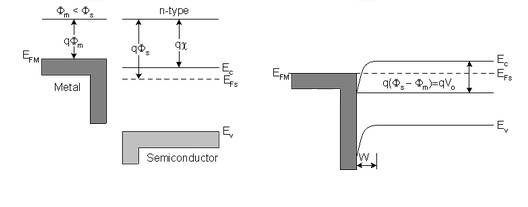
Here in below figure we can see an ohmic contact formation between a metal and n-type semiconductor .
Untitled_zps36e0b9cf.jpg


Here how the N-type semiconductor bands are banded upward ?
and what type of depletion charge exists there ?
 
Last edited:
Physics news on Phys.org
  • #2
electrons will flow into the semiconductor from the metal until enough negative charge has accumulated in the semiconductor to give an electric field strong enough to stop the flow of charge. The electric field comes from the semiconductor having a net negative charge (where before it was neutral). The bands are bent whenever you have a non-zero charge density. Electrons are depleted from the metal and accumulated in the semiconductor.
 

Related to Depletion region in n-type ohmic contact

What is a depletion region in n-type ohmic contact?

A depletion region in n-type ohmic contact is a region in a semiconductor material where the concentration of free charge carriers is significantly reduced due to the presence of an electric field. This is caused by the diffusion of dopant atoms from the contact into the semiconductor material.

Why is the depletion region important in n-type ohmic contact?

The depletion region plays a crucial role in determining the electrical properties of a semiconductor device. It controls the flow of current between the contact and the semiconductor material, and affects the overall performance and efficiency of the device.

How does the depletion region form in n-type ohmic contact?

The depletion region forms when an n-type semiconductor material, which has an excess of free electrons, comes into contact with a metal that has a higher concentration of dopant atoms. The dopant atoms diffuse into the semiconductor material, creating a region with fewer free electrons.

What factors influence the size of the depletion region in n-type ohmic contact?

The size of the depletion region is influenced by the concentration of dopant atoms in the metal contact, the type of semiconductor material, and the applied voltage. A higher dopant concentration, a wider bandgap semiconductor, and a larger applied voltage will result in a larger depletion region.

How does the depletion region affect the electrical characteristics of n-type ohmic contact?

The depletion region acts as a barrier to the flow of current between the contact and the semiconductor material. As the size of the depletion region increases, the resistance of the contact also increases, leading to a decrease in the flow of current. This can affect the overall performance of the semiconductor device.

Similar threads

Replies
3
Views
5K
  • Atomic and Condensed Matter
Replies
2
Views
2K
  • Atomic and Condensed Matter
Replies
7
Views
690
  • Atomic and Condensed Matter
Replies
1
Views
1K
  • Atomic and Condensed Matter
Replies
1
Views
2K
  • Atomic and Condensed Matter
Replies
1
Views
2K
  • Atomic and Condensed Matter
Replies
1
Views
2K
  • Engineering and Comp Sci Homework Help
Replies
1
Views
602
  • Atomic and Condensed Matter
Replies
6
Views
2K
  • Atomic and Condensed Matter
Replies
0
Views
128
Back
Top